Application example: Laser-assisted bonding
The LASCON system enables the gentle machining of sensitive componentsMergenthaler has been a renowned supplier of laser systems and components for laser-assisted bonding for decades.
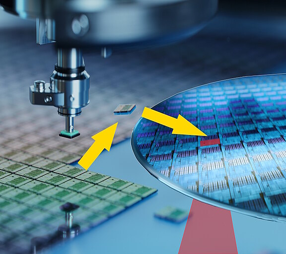
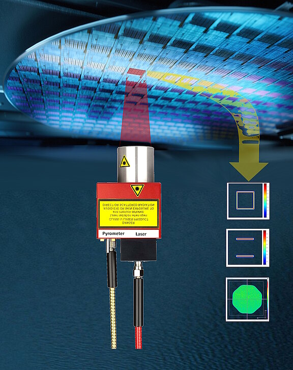
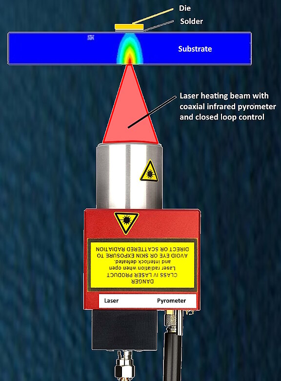
In laser-assisted bonding, the key benefit for the individual processing of small components is that the laser energy results in minimal, locally confined heat input. Rapid heating rates, monitored by a pyrometer, prevent surface oxidation and lead to short production cycles for individual components. Even with fully populated substrates, each component can be processed individually without affecting neighbouring components. Due to the low thermal load, the thermal expansion of the substrate is negligible and the positioning accuracy of the components is improved.
Well-known packaging processes such as chip-on-submount (CoS), chip-to-chip (CoC), chip-on-wafer (C2W) and others can be carried out using laser-assisted bonding.
Laser components from Mergenthaler are also used for the packaging of photonic components, such as for laser-fibre coupling, optical device packaging in general, die bonding, flip-chip bonding or eutectic bonding (laser brazing). Laser drying is also possible.
Depending on the type of substrate, the process can be carried out in two different ways. If the substrate is transparent, the solder is melted directly. If the substrate is absorbent, it is heated from the underside, and the heat is conducted through the substrate to the solder.
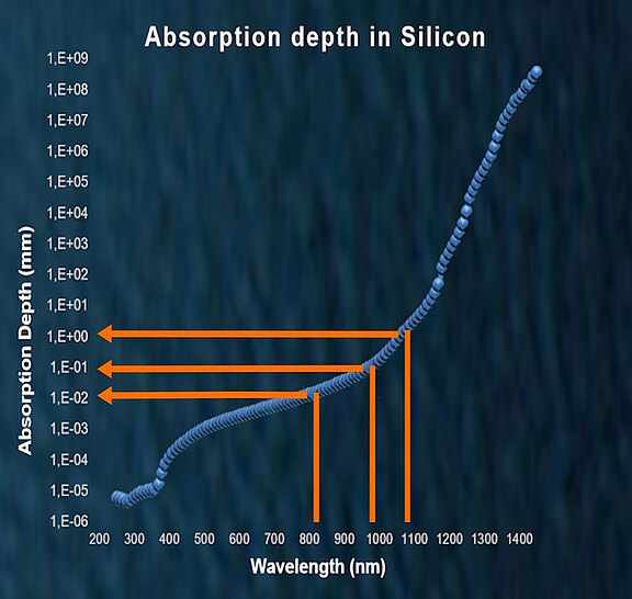
If the substrate is a silicon wafer, absorption depends on the wavelength of the laser. If the spectral transmission curve of the silicon wafer is known and a suitable laser wavelength is selected, various effects can be achieved. The heat can be absorbed at the bottom surface, within the volume of the substrate, or at the top surface of the substrate.
The diagram below shows the absorption depth of pure silicon as a function of wavelength.
- For a laser wavelength of 808 nm, the absorption depth is approximately 0.01 mm.
- For a laser wavelength of 975 nm, the absorption depth is approximately 0.1 mm.
- For laser wavelengths between 1064 nm and 1080 nm, the absorption depth is approximately 1 mm.
By absorption depth, we mean the distance after which the laser power is still 37 per cent of its initial intensity.
If the silicon wafers are doped, the absorption behaviour may change and the spectral transmission should be measured.
If the substrate is metallised, a laser with a blue wavelength (450 nm) should be considered for heating.
Blue light is absorbed significantly better here than the light from NIR diode lasers.
If the metallisation consists of gold, the blue laser is the only sensible alternative.
MERGENTHALER offers high-brightness blue lasers with laser powers of up to 100 W in a 200 µm fibre – air-cooled!
Discuss your ideas with our team of engineers and benefit from over 30 years’ experience in laser technology.